Acrylic: More properly Poly(methyl methacrylate) or PMMA is a thermoplastic and is transparent. It is a polymer of methyl methacrylate CH2=C(CH3)CO2CH. It is sold under many names including plexiglass, lucite, acrylic glass, simply acrylic. It is often used as an alternative to glass or the more expensive due to its low cost and easy handling and processing. However, it is not very shock resistant to impact forces.
Alloy: a material made up of two or more elements where the atoms are “dissolved” into each other very much like a liquid solution of salt in water. However, alloys are solid so what this means at the atomic level is that the atoms of the different elements are geometrically packed in a regular crystalline manner but their identity changes randomly. Everyday examples of alloys are steel (iron and a little carbon), bronze (copper and tin), and gold and silver in jewelery (each allowed with traces of different metals to give them strength).
Carrier recombination: The process by which electrons and holes in semiconductors annihilate in pairs to release energy. Read more about it here.
Curie Temperature: the temperature above which magnetism is destroyed in a ferromagnet. Above this temperature, the electron spins in the ferromagnetic material no long want to point in the same direction. Different materials have different Curie temperatures: e.g. for iron it is 770 degrees Celcius while for nickel it is 358 degrees Celcius.
Dielectric constant: is a measure of how strongly a material polarizes in response to electric fields and hence how much it reduces the strength of the field applied to it when compared to the same field in vacuum. When an external electric field is imposed on an insulator, the charges in the material can not flow freely but they can shift in position and thus polarize. Positive charges move in the field direction and negative charges in the opposite direction. The dielectric constant is a quantitative measure of how much a material polarizes for a given strength of electric field. Since polarization means charges have displaced, and charges create electric field, the polarization itself will create fields as well and a moment of thought shows that they will be in a direction to oppose the applied external field. In the net, the actual field in the material (sum of external plus internally generated field from the polarization) is reduced. Precisely, it is reduced by a factor equal to the dielectric constant, which from this definition should be positive and larger than one. Some examples: the dielectric constant of glass is between 3 and 4, that of silicon is 12, for water at ambient conditions it is close to 80, and for air it is very close to one (1.00058986), and is 1 for vacuum by definition. As a technical note, normally the term “dielectric constant” refers to the response of a material to a constant (in time) electric field and a more precise term for this is the static dielectric constant. This is because one could put a time-dependent external electric field on the material and thus induce a time-dependent polarization. As the frequency of the external field is varied, the charges in the material (free ions, electrons free or bound, nuclei, etc.) respond differently and in a dynamic way. Thus one can generalize the concept to a frequency dependent dielectric function.
Diode: The simplest semiconductor device whereby two oppositely doped semiconductors are placed in immediate contact. Among its many properties, the diode acts as a one-way street, allowing current to flow through it most easily only in one direction. Read more about diodes here.
Doping: The process of adding trace amounts of foreign atoms to a semiconductor in a controlled manner in order to tailor its conductivity. Read more about this process here.
Electron spin: Electrons are fundamental particles, i.e. fundamental building blocks of matter. In atoms, they orbit the positive nucleus and form atomic shells. Aside from their negative charge, electrons possess another property called spin, which is in fact a purely quantum phenomenon. Pictorially and loosely speaking, what this means is that electrons are like spinning tops and thus have angular momentum. What is peculiar and quantum mechanical is that the amount of angular momentum (the rate of spinning) is fixed; only the direction can be changed. This picture is illustrative and can not be taken literally since (as far as we know) electrons are point particles and it is hard to imagine an object that is spinning but has no spatial extent — again quantum mechanics can be counter-intuitive. Since electrons are charged and spinning, they must act like tiny bar magnets and have a magnetic moment. Their tiny magnetic moment is only 9.28 x 10⁻²⁴ Amps x m2. What this means is that in addition to having charge and thus creating electric fields, electrons are like tiny bar magnets that create magnetic fields too! The magnetic moment and magnetic field, just like the charge and electric field or the mass, are instinsic and part of what an electron is. Separately, this spin magnetic moment is completely separate and distinct from any magnetic moment the electron generates due to its motion (called orbital magnetic moment) say due to its orbit around the nucleus.
Ferromagnet: a material that likes to become magnetized on its own under normal circumstances. The prefix “ferro” means iron, one of the oldest magnetic materials known to man. Ferromagnetic materials, like iron or nickel or cobalt, have the property that their lowest energy (most stable) state has magnetization — the electron spins in the material like to become aligned in the same direction. Each electron is a small bar magnet, but with huge numbers of them pointing in the same direction, a large and macroscopic magnetization and magnetic field can be created. When ferromagnets are heated to high temperatures, the electron spins start flopping around due to thermal fluctuations and no longer point in the same direction; the magnetism gets smaller and ultimately disappears when the Curie temperature is reached. Each magnetic material has its own Curie temperature (e.g. 770 degrees Celcius for iron).
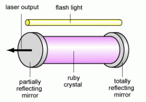
 Ruby laser (schematic) |
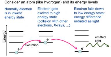
 Schematic showing how an atom will be excited and then de-excite by emitting light Schematic showing how an atom will be excited and then de-excite by emitting light |
Laser: The word laser is actually an acronym for Light Amplification by Stimulated Emission of Radiation. The user of the word light is in the broad sense of electromagnetic radiation in general and not necessarily only the visible spectrum. Lasers exist that create radiation in the infrared, visible, ultraviolet, and even X-ray regions. Lasers emit radiation by a process based on stimulated emission, a physically different process from ordinary light sources such as lamps or bulbs which is based on spontaneous emission. Generally speaking, light is created when an atom or a molecule has electrons in high-energy (excited) states that then relax to their lower energy native states (ground state) and release the energy in the form of a quantum of light (photon). In a given material, there are many excited atoms or molecules so many photons are emitted. Spontaneous emission is the simplest version: each atoms or molecule radiates its photon independent of the other radiative events and there is no correlation. So while the frequency of all the photons are the same and determined by the energy difference between the excited and ground state, their phase is not correlated, i.e. the crests of the different waves do not align with each other but are randomly shifted with respect to each other. In stimulated emission, the photon emitted by one radiative event stimulate (“tickles”) the next atom or molecule to emit and furthermore to emit in lock-step; the process is like an avalanche with each emission stimulating the next one and thus one gets a large number of photons emitted with aligned crests (well-defined phase relation). This means the radiation emitted is coherent. To have stimulated emission, the number of excited atoms or molecules must be large so that an emitted photon has a high chance or running into another excited atom or molecule before exiting the sample. This large density of excitation is called population inversion: more atoms or molecules are in the excited state than the ground state. Obviously, energy must be supplied to create so much excitation, and that is the energy a laser consumes to produce its radiation. Finally, to enhance the entire process, the emitting material is placed in a optical cavity such as between two mirrors: that way, the photons bounce between the mirrors and thus make multiple passages through the material thus enhancing the chances of creating stimulated emission. The picture to the right shows a schematic of a classic ruby laser. The pink region is the body of the laser (the active material) where the excited atoms emit photons. The atoms are excited by the flash lamp which supplies the energy to drive the laser. Two mirrors at the ends form the optical cavity which make the photons bounce back and forth through the material to enhance stimulated emission. One mirror is partly reflecting to allow some of the light to “leak out”: this is the actual laser output radiation.
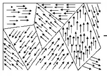
 Magnetic Domains |
Magnetic domain: while a ferromagnet likes to magnetize below its Curie Temperature, this does not mean that all the electron spins in the entire material will all point in the same direction. Rather, what happens in reality is the magnetic pattern is a patchwork of different subregions of the material inside of which all the spins point in the same direction but the different subregions have independent directions of the magnetization. The figure on the right illustrates this: the arrows are supposed to represent the directions of electron spins. Each subregion where the spins align together is called a magnetic domain. When the magnetic domains all have magnetization pointing in different directions, the net magnetization of the material is very small or zero — although the material likes to magnetize, it has no net magnetization. To magnetize the material is easy: external magnetic fields create forces on electron spins that like to align their spin direction (arrow in figure) with the direction of the external field. So the external field will flip or align some of the spins preferentially and, in the net, more spins will be pointing along the external field: a net magnetization has developed. Another way to say this is that domains whose magnetization is aligned with the external field are preferred, grow in size, and outnumber other domains that are aligned otherwise. Once the external field is removed, the net magnetization can remain for a very long time as the rate of motion of the domain boundaries and the flipping of spins can be very slow (i.e. years) — although this depends on the type of magnetic material and its preparation.
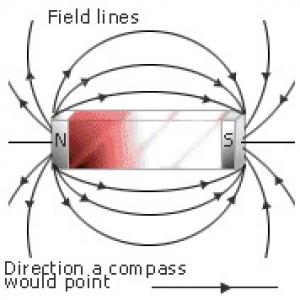
 Dipolar field pattern of a bar magnet |
Magnetic moment: the quantitative measure of the strength of any system creating magnetic fields (a bar magnetic, a current loop, an electron spin, etc.) The SI units for magnetic moment are Amps times m2. Thus a circular conducting wire where one Amp flows with area of one m2 has one unit of magnetic moment. Larger magnetic moments create proportionally larger magnetic fields. The magnetic moment is actually a vector so it has a head (north pole) and a tail (south pole) and for purposes of computing its magnetic field, is exactly like a bar magnet: fields emanate from the north pole and terminate at the south pole. Two systems with the same magnetic moment when viewed from afar create the same magnetic field pattern. The picture on the right shows an illustration of a bar magnet creating a dipolar magnetic field pattern; however, please note that any magnetic dipole creates such a field pattern and this is not restricted to bar magnets.
MOSFET transistor: The Metal Oxide Field Effect Transistor, the most common type of transistor manufactured today. The transistor is a semiconductor device that acts like a switch where one voltage controls the flow of current in other parts of a circuit in an on-off manner. Read more about it here.
Photodiode: This is a photodetector. When light is absorbed by a photodiode, it generates an electrical signal (either a current or voltage depending on the details). Thus it is a light to electricity converter. Internally, it is made of two semiconducting materials that touch (a p-n junction to be precise): when light is absorbed in the junction region, mobile electrons are created which they give rise to the measured electrical signal.
Polymer: Polymers are molecules built from taking many copies of a relatively short molecule and stringing them together into one very long molecule (i.e. a long chain with many links). In this sense, a polymer can become arbitrarily long; the longer the polymer, the heavier it is and thus the higher its melting point and the more viscous it acts (usually). The name comes from the Greek polumeros (having many parts) which is built from the root polu- (many) and meros (a share or part). Many organic molecules are polymers such as fats or proteins.
Polycarbonate: A particular type of plastic, or more precisely a thermoplastic polymer. They are easily worked, molded, melted, and remolded and thus are very useful in industrial applications. They also have excellent resistance to temperature and impact and are generally very optically transparent. Polycarbonates derive their name from the fact that their units are joined together by carbonate bonds: in chemistry the carbonate ending of a molecule is COOH; in polycarbonates, the H is removed and the C acts like abridge with oxygens on two sides in the form -O-C-O- gluing one unit to the next (there is a double-bonded O attached to the C so the more proper notation would be -O-(C=O)-O).
Scanning Electron Microscope (SEM): A microscope that images by scanning with a high-energy beam of electrons. The electrons interact with the atoms of the sample in a variety of ways: they can knock out other electrons (secondary electrons) that fly away from the sample and are detected, they can bounce of the sample (back-scattered electrons), they can cause the sample to emit X-rays characteristic of the materials making up the sample, they can cause the material to emit visible light, etc. In principle all these signals could be used to image the sample, but in practice only a few are for practical reasons. Most common on the secondary electron detectors which give high resolution images (typically down to 1-2 nm) of the topography of the sample surface. Many of other signals (e.g. back-scattered or X-rays) provide information about the elements composing the material.
Semiconductor: A material that in its native form is a good insulator but which can be made into a conductor by controlled addition of trace amounts of foreign elements, a process called doping. Silicon is the most widely used semiconductor. For more details on semiconductors go here.
Semiconductor laser: A semiconductor laser or laser diode is a type of laser. In such a laser, the active medium is a semiconductor similar to that found in a light-emitting diode (LED). The most common and practical type of laser diode is formed from a p-n junction and powered by injected electric current. These devices are sometimes referred to as injection laser diodes.
Spin: see electron spin above.
Transistor: The most common basic electronic device manufactured today. While there are many types of transistors, the most common one is the MOSFET transistor.
Transmission electron microscope (TEM): this is a technique for microscopy (viewing very small things) that uses a beam of electrons that are shot through the sample being analyzed. The electrons pass through the sample (which should be very thin, otherwise most of the electrons are scattered or absorbed and few are transmitted) and interact with the sample during the passage. After they emerge, they are focused down to form an image which shows a magnified view of the material. Advanced TEM machines can routinely resolve features with sub-nanometer dimension and thus allow individual atoms to be seen in a sample; additional analysis can even reveal the atomic species present.
Thermoplastic: This is a type of plastic that turns liquid when heated and thus can flow and thus be molded, remolded, or remelted into shape. When cooled, it becomes an extremely viscous fluid (and is solid for practical purposes at room temperature).