This page has multiple sections. Each section can in principle be read in isolation, but it helps to know the preceding material to fully understand the next one. The below contents are under these topics:
- Semiconductors
- Doping
- Diodes
- Carrier recombination
- Carrier photo-generation: the basis for (semiconductor) solar cells
- The transistor
- MOSFET transistor (metal oxide field effect transistor)
Semiconductors
A semiconductor is a material that in its pure (native) form is a good insulator (i.e. a poor conductor) but which can be made into a conductor via the controlled addition of a very small percentage of foreign elements through a process called doping (see below). Typical semiconductors that are widely used today are silicon (Si), germanium (Ge), gallium arsenide (GaAs), perhaps the alloy of silicon and germanium (SiGe), as well as the family of nitrides including indium nitride (InN), gallium nitride (GaN), and aluminum nitride (AlN) and their various alloys where the In/Ga/Al are mixed in various proportions with nitrogen.
Not all materials that are insulator make good semiconductors. The materials must be special in the sense that one can control their conductivity precisely via doping. And, of course, one must have advanced enough materials processing and technological know how to do this. Both the choice of materials and the necessary technology are reasons why the transistor was invented in the middle of the 20th century and not the late 1900s. The main enabling materials are semiconductors.
Doping
The controlled addition of foreign atoms to a semiconductor to change its conductivity is called doping. Let’s proceed by example. Silicon is the current materials underlying all modern electronics. But silicon in pure form is actually an insulator under ambient conditions: all the electrons in pure Si are bound up in strong chemical bonds between the Si atoms and can not move around freely. However, if a very small percentage of phosphorus or boron is introduced into silicon, it can become conducting. It is this addition of controlled amounts of foreign atoms like phosphorous or boron that is the doping.
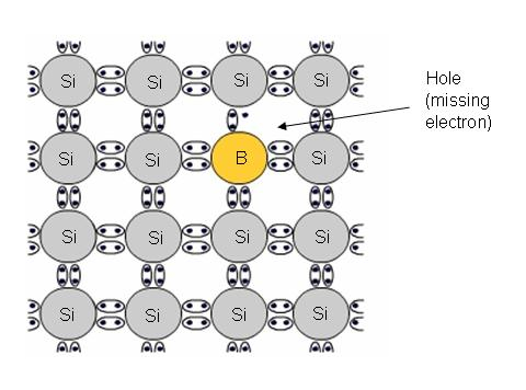 Boron doping in silicon Boron doping in silicon |
Small means that at most one out of ten thousand (more typically 1 out of a million or so) of Si atoms are replaced by P or B (or other elements). Therefore, the material is still basically silicon except for a rare intruders (dopants) appearing here or there. But even such a minuscule number of foreign atoms has a dramatic effect on the conductivity. In the case of P, because P is to the right of Si on the periodic table, it has one more outer (valence) electron than Si. Therefore, as a dopant, each P atom replaces a Si atom but because it has one too many electrons, it donates that electron to the material. This means amobile electron has been added that can freely wander about the material. The set of mobile electrons are then the moving charges that make P-doped silicon conducting. For boron, things are backwards: B is to the left of Si on the periodic table so it has one fewer outer electron. When B replaces Si in the crystal lattice, the boron atom binds an electron (i.e. steals an electron from the other silicon atoms), and this missing electron — called a hole — wanders around freely instead. Doping with atoms that give electrons (like P for Si) is called electron doping or “n-type” doping in the semiconductor literature, and the converse which is hole doping is called “p-type”. Regardless of type dopant (n or p), the point is to introduce mobile charge into the otherwise insulating material. The figure on the right shows the example of boron doping in silicon: a Si atom has been replace by B and there is an electron missing from one of the bonds (from basic chemistry, normal bonds have two electrons per bond represented by the two dots).
What is remarkable about semiconductors and doping is the amazing control provided over the process. For low to medium levels of doping, the number of added mobile charges is directly proportional to the number of dopants added: so with carefully controlled material engineering, one can make a new material with some desired level of conductivity (within certain limits, of course). To fully appreciate why this is remarkable, notice that having conductors is no big deal: any good metal, such as copper or gold or silver, is a conductor. But one can’t change the conductivity of a given material like copper in a quantitative and controlled way — in some sense the material properties are “God given”: copper has some conductivity as determined by its atomic nature and how the copper atoms bond together when forming the metal. With semiconductors, one has an entire class of artificial materials whose conductivity is tunable.
A wide variety of materials are semiconductors and can be doped. But only a few can at present be produced in mass and in highly reliable form for industrial production. The first transistors were made of germanium (Ge), but Si is the current material of choice. For certain applications requiring high performance gallium arsenide (GaAs) is used or perhaps the alloy of silicon and germanium (SiGe).
Diodes
A diode is the simplest possible semiconductor device. As explained in more above, one can dope the semiconductor to have either extra electrons that are mobile and can cause conduction (called an n-type semiconductor) or one dope it to have too few electrons — the missing electrons are called holes — so that the conductivity is due to the holes (which are positive since they are missing negative charge) moving around (a p-type semiconductor).
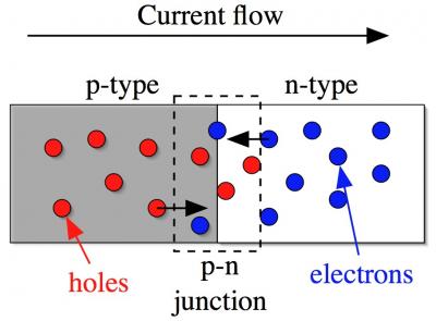 Diode schematic Diode schematic |
A diode is made by placing an n-type and a p-type semiconductors in direct physical contact. The region where they meet is called the p-n junction. On the right is a schematic of the basic diode geometry. We have a gray shaded region on the left which is the p-type semiconductor: the holes are shown are red balls. On the right is the n-type material with white background: the electrons are shown as blue balls. The junction region is indicated by the dashed box.
What is interesting about diodes is that they are clearly asymmetric: both parts of the ensemble are conducting but the left portion has holes whereas the right side has electrons. What this translates into is that the conduction through the diode is asymmetric as well: current flows easily from left to right but not easily the other way. Put another way, the diode is a one-way street for current. The direction of easy flow is from left to right for the diode in the schematic: holes move to the right and electrons move to the left. Therefore, holes and electrons will both be arriving in the junction region when a current is made to flow. The current is created by a voltage source, such as a battery, the puts a voltage across the two ends of the diode. This asymmetry is already a very useful thing and makes diodes enormously useful in electronic and electrical applications.
Carrier recombination
Now consider in more detail what happens in a diode when, say, and electron from the n-type region moving leftwards enters the p-n junction region and wanders into the p-type material. In the p-type material, there are many missing electrons and thus the newly introduced electron has the possibility to fill one of these missing slots. And in the process it loses energy — pictorially the electron finds a hole and “eats it up” releasing energy (or in more fancy language the electron and hole annihilate each other. The converse process works as well: a hole that moves to the right and enters the n-type region represents a missing electron, so one of the many extra electrons in the n-type material can fill up that hole. This process of electrons “eating up” the holes is called carrier recombination: the two types of mobile charges recombine into the native state of the material (an excess electron and a missing electron combine to make nothing extraordinary giving up energy in the process).
As you can see, the details might be different, but basically the diode creates a physical situation where once a current is made to flow, electrons end up in a situation where they can enter lower energy states and release energy. One has turned the electrical driving energy (from a battery, for example) into energy liberated by electrons dropping into lower energy states. All one has to do is now harness that liberated energy. Unless one has designed things properly, this liberated energy is generally lost into heat. However, with the right choice of materials, this liberated energy can be turned into light which underlies the Light Emitting Diode (LED).
Carrier photo-generation
The opposite process to recombination in an LED is also possible: light can be captured by a diode and turned into an electron+hole pair. This is charge carrier creation, the opposite process of recombination. In fact, all diodes are sensitive to light in this manner, and the created electron+hole then lead to a current. In most circuits, this is undesired behavior so the diode is clad in a light-absorbing casing. However, this is obviously very useful for two application: (1) where one wants to detect light which means one has a photodiode, and (2) where one wants to harvest the current as electrical energy so one is using the diode as part of a solar cell(photovoltaic device). As you can imagine, one must choose materials and processing carefully to optimize the diode for each particular application.
The transistor: the modern day marvel
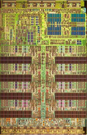 Top view (false color) of the Playstation 3 chip Top view (false color) of the Playstation 3 chip |
Without serious argument, the transistor is one of the most important and life-altering inventions of the 20th century. It underlies all of electronic processing and has made the entire information and computer revolution possible. In fact, it use pervades almost every aspect of modern life as all electronic devices, no matter how primitive, are based on transistors. This encompasses computers, cellular phones, modern televisions, digital music players, controllers of all sorts (CD or DVD players, hard drives, automatic brakes on cars), microwave ovens, video game machines, bank teller machines, digital watches, and this list goes on for a very long time. Anything which does any type of digital computation or information manipulation uses transistors. Transistors are so pervasive that it is really hard to know where they are to be found in every day life.
To give you a feeling for the staggering scale of transistor production, consider the following fact: in 2006, 60 million transistors were created for every living person on Earth. That is 4 x 10¹⁷ transistors! (400 quadrillion for those who like big names for large numbers.) By 2014, the number should close to 2 x 10²⁰ (200 quintillion) (Reference). Typically, very large numbers of transistors are packed densely together on integrated circuits to make the “computer chips” that are inside many devices; a modern processor has about a billion transistors in it. On the right is an image of the Playstation 3 microchip viewed from a reasonable magnification: here, one is mainly looking at the wiring, which looks quite complicated. And indeed, as you can imagine, wiring up a billion transistors to do different things on one chip (do arithmetic, logical operations, access memory, keep track of time, move data around, etc.) is a complex engineering feat.
The next image shows a closeup of the wiring of an older chip (circa 1997). We don’t see the transistors just yet, but we are still mainly looking at the individual wires that go to the transistors and connect them to each other. This is an SEM image from IBM using their copper interconnect technology invented in 1997. The widths of the wires are close to 0.2µm or 200 nm. That such wiring can be laid down on so many levels with such precision to connect such enormous numbers of objects is a stupendous achievement in modern technology — one we are generally unaware of or take for granted.
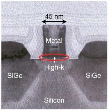 TEM image of a single transistor from Intel’s 45nm technology TEM image of a single transistor from Intel’s 45nm technology |
Finally, to the right is a very high resolution TEM image of a single transistor viewed from the side. This is a recent transistor from Intel’s 45 nm technology — the number refers to the lateral size of the transistor as shown in the figure. The precise arrangement of materials and their function is described in the next section on the MOSFET. The transistor’s main action is actually confined to a very narrow region in the entire device that is circled red in the diagram. This is the region between the semiconductor (Si here) and the oxide (high-k here).
MOSFET transistor
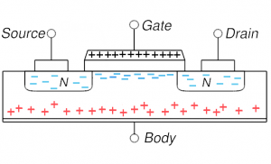
Almost all transistors manufactured today are MOSFET transistors: Metal Oxide Semiconductor Field Effect Transistors. On the right you see a schematic of a MOSFET.
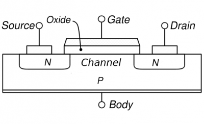 MOSFET schematic MOSFET schematic |
The source, drain, channel, and gate are all conducting materials. The gate, typically a metal, is separated from the rest of the materials by the oxide which is insulating. Silicon dioxide in the older technologies but a “high-k” material as in the above Intel 45nm TEM image in modern transistors; high-k materials used today refer to oxides of transition metals such as hafnium or zirconium with perhaps some silicon added; “high-k” means they have a large dielectric constant. The source, drain, and channel are semiconductors. For the MOSFET pictured on the right, the source and drain are n-type while the body is p-type; the converse is also possible (p-type source and drain and n-type body). The main point is that the body is always doped oppositely to the source and drain. See the end of the text for the difference between these to possibilities.
To put it most simply, a transistor is a switch. You can turn it on or off with a voltage. More precisely, you can make it conducting or highly insulating depending on the voltage you put on it (on the gate). The basic operation is as follows: a voltage is applied across the source and drain in an attempt to make current flow between them. However, whether this happens or not depends on the voltage applied to the gate: the gate controls the conductive properties of the channel (the region between the source and drain in the picture). Thus changing the voltage on the gate changes the conductive properties of the channel and thus the current between source and drain. In this way the transistor can be used as a switch: a lot of current or little current can be made to flow depending on the state of the gate.
But how can material conductivity be controlled in this way? What makes the channel material special? Or do all materials behave this way? The answer is that in fact the materials must be special, which is part of the reason the transistor was invented in the middle of the 20th century and not the late 1900s. The main enabling materials are the semiconductors described above.
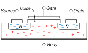 MOSFET: no gate voltage and the natural distribution of holes throughout the body MOSFET: no gate voltage and the natural distribution of holes throughout the body |
 MOSFET in accumulation: negative gate voltage attracts holes and they accumulate in the channel region MOSFET in accumulation: negative gate voltage attracts holes and they accumulate in the channel region |
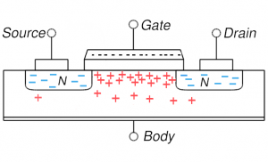
 MOSFET in depletion: positive gate voltage repels holes and the channel region is depleted of holes MOSFET in depletion: positive gate voltage repels holes and the channel region is depleted of holes |
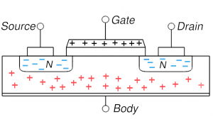
 MOSFET in inversion: very positive gate voltage repels all holes and actually attracts electrons (from source and/or drain) into the channel; the p-type region in the channel has been inverted in doping MOSFET in inversion: very positive gate voltage repels all holes and actually attracts electrons (from source and/or drain) into the channel; the p-type region in the channel has been inverted in doping |
On the right, four key cases are shown for the MOSFET described above. Concentrate first on the upper left which shows the distribution of electrons and holes when nothing is done (no voltages applied): the n-type source and drain have mobile electrons (blue minuses) and the p-type body has holes. If you try to run a current from source to drain through the body, there as essentially two diodes back-to-back: the first going from source to body and the next from body to drain. And the two diodes have opposite orientation so if one can flow current easily the other can’t. Basically, this situation is highly resistive and not much current can flow (we can say the MOSFET is off). One can make sure of this resistive behavior and increase the resistivity by putting a negative voltage on the gate (upper right): this is accumulation mode where holes are attracted into the channel region making for even stronger diode behavior and more resistive behavior.
On the other hand, if one puts a modest positive voltage on the gate, holes are driven away: this is shown in the lower left and is depletion mode (channel is depleted of its native mobile charges, the holes). This setup is now more conductive as the diode behavior has been reduced. But almost all MOSFETs are operated in the more extreme situation of inversion: the positive voltage is increased to the point that not only are all holes driven away from the channel, but some electrons (from source and or drain) enter into the channel region. The thin channel region is now n-type (has been inverted). We now have n-type material connecting source and drain and thus no diode behavior and a very highly conductive state. Current flows easily from source to drain.
Basically, when a MOSFET is used as a switch, it is used in inversion (conductive or on) or with little or weak negative voltage (accumulation). This makes the source-drain connection either very conducting or highly resistive. The electric fields created by the gate repel or attract conducting charges: hence the “field-effect” part of the MOSFET name.
An important fact to note is that the MOSFET is volatile: it forgets its state if power is removed. For example, if the conductivity or resistivity of the channel is encoding information, the gate voltage has to be applied and kept being applied — if it is removed, the transistor forgets that it was applied and forgets its state. Therefore, as such, the MOSFET can not be used to store information permanently (or semipermanently) without continuous power consumption to maintain the gate voltage.
A final note about the two choices of doping, i.e. whether the source and drain are n-type and body p-type or vice versa. For n-type source/drain, we have a nMOSFET while the opposite is a pMOSFET. The two have identical principles governing their function except that all the voltages are reversed: an nMOSFET is in inversion and thus “on” or conducting for positive (high) voltages and “off” or resisting for negative (low) voltages. A pMOSFET is exactly the opposite: “on” for low voltage and “off” for high voltage.